混合卤素CsPbBrxI3–x钙钛矿量子点具有良好光谱可调性,在纯红光钙钛矿发光二极管领域中具有良好的应用潜力。然后,该类量子点面临着表面缺陷和不稳定性这两大难题,严重阻碍了其在高性能器件中的实际应用价值。
基于此,郑州大学张继斌研究员与华中科技大学屠国力教授等人报道了采用钇阳离子(Y3+)掺杂和苯基膦酸(PPA)钝化的协同策略来解决这些问题。其中,引入Y3+离子掺杂后,量子点的形成能得以降低,而碘化物空位缺陷的形成能则有所增加。PPA则通过其膦氧化物基团与未配位的 Pb2+离子配位,成功实现了对表面缺陷的有效钝化。并且,PPA的羟基还能与相邻卤素离子形成氢键,抑制了卤素离子的迁移,进一步增强了钝化效果。
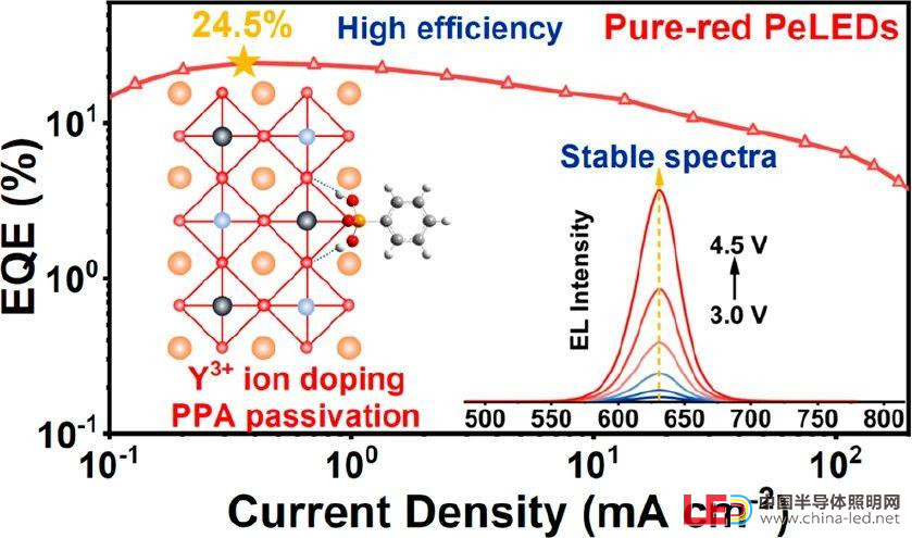
最终,Y/PPA 共改性量子点表现出了卓越的稳定性,光致发光量子产率近乎达到100%。基于这些量子点的钙钛矿发光二极管具有出色的光谱稳定性,外量子效率达到24.5%,是基于 CsPbBrxI3–x量子点的纯红光钙钛矿发光二极管效率最高者之一。
该工作得到了国家重点研发计划、国家自然科学基金、中国博士后科学基金等项目资助。
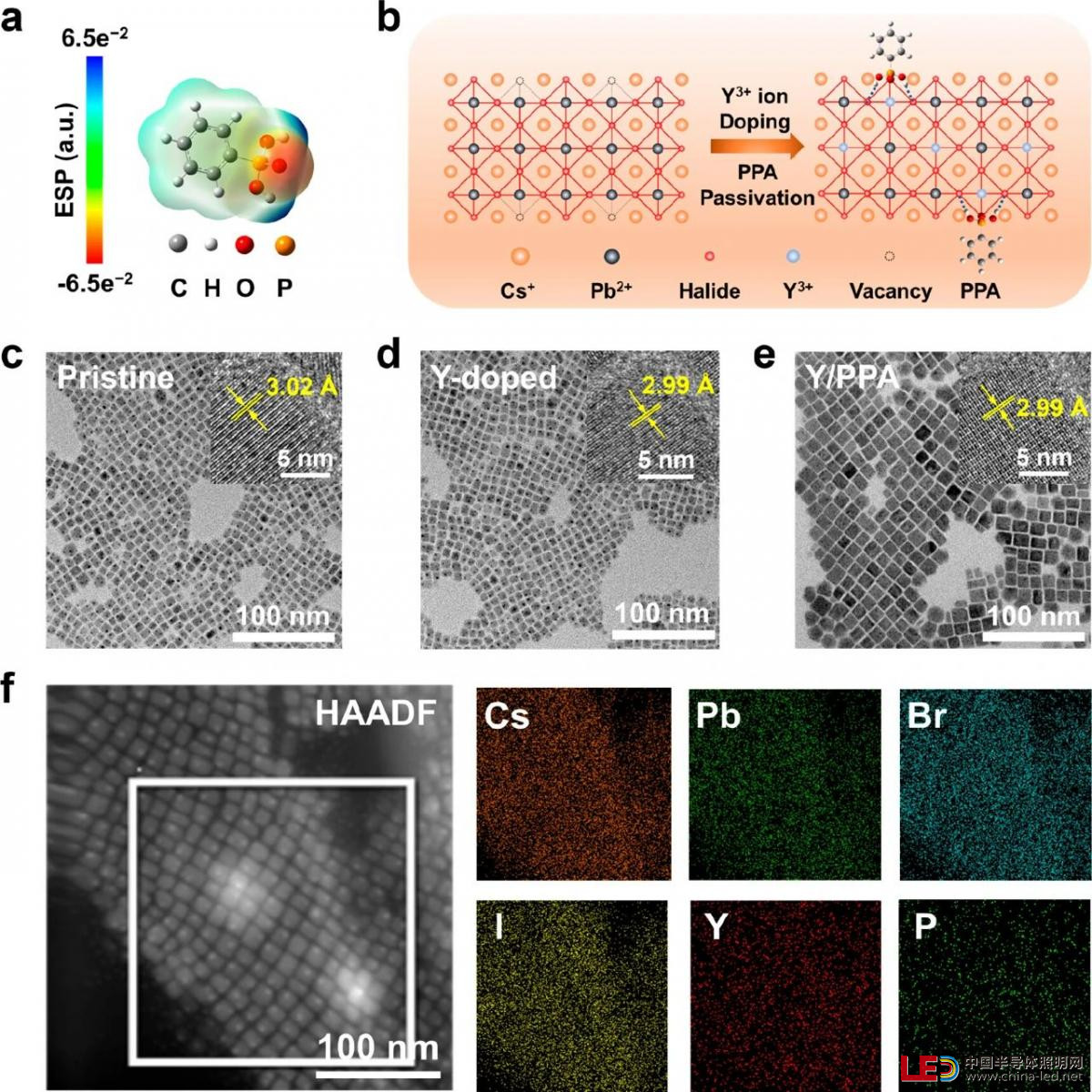
Figure 1. (a) Electrostatic potential (ESP) map of PPA molecules. (b) Schematic illustration of CsPbBrxI3-xNCs before and after synergistic modification of Y3+ ion doping and PPA passivation. TEM images of (c) pristine, (d) Y-doped, and (e) Y/PPA NCs. The insets show corresponding HRTEM images. (f) Elemental mapping images of Y/PPA NCs.
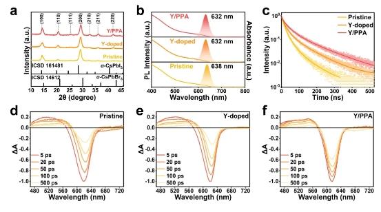
Figure 2. (a) XRD patterns, (b) PL and Absorption spectra, (c) Time-resolved PL decay curves of pristine, Y-doped, and Y/PPA NCs. TA spectra of (d) pristine, (e) Y-doped, and (f) Y/PPA NCs at different probe delay times.
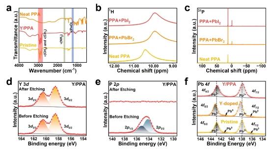
Figure 3. (a) FTIR spectra of pristine NCs, Y/PPA NCs, and neat PPA. (b) 1H and (c) 31P NMR spectra of neat PPA, a mixture of PPA and PbBr2, and a mixture of PPA and PbI2 in dimethyl sulfoxide (DMSO-d6) solution. High-resolution XPS spectra of (d) Y 3dand (e) P 2p of Y/PPA NCs before etching and after etching. (f) High-resolution XPS spectra of Pb 4f of pristine, Y-doped, and Y/PPA NCs.
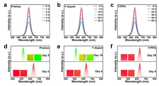
Figure 4. PL spectra of (a) pristine, (b) Y-doped, and (c) Y/PPA NC films at different times (photostability test: under UV light continuous irradiation). (d) PL spectra of pristine NC films on day 0 and day 5 (stability test: 40 ℃ and 80% RH). The insets show the corresponding photographs of pristine NC films under daylight (left) and UV light (right) on day 0 and day 5. (e) PL spectra of Y-doped NC films on day 0 and day 16 (stability test: 40 ℃ and 80% RH). The insets show the corresponding photographs of Y-doped NC films under daylight (left) and UV light (right) on day 0 and day 16. (f) PL spectra of Y/PPA NC films on day 0 and day 29 (stability test: 40 ℃ and 80% RH). The insets show the corresponding photographs of Y/PPA NC films under daylight (left) and UV light (right) on day 0 and day 29.
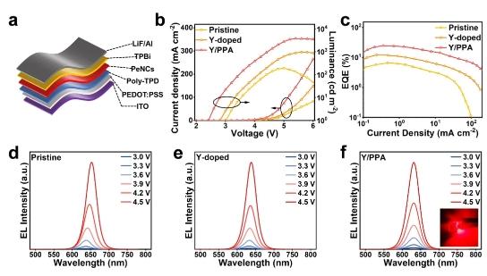
Figure 5. (a) Device structure of PeLEDs. (b) Current density−voltage−luminance curves of PeLEDs. (c) EQE−current density curves of PeLEDs. EL spectra of PeLEDs based on (d) pristine, (e) Y-doped, and (f) Y/PPA NCs at different bias voltages. The inset shows a working PeLED.
